The New AI Bottleneck: How Advanced Packaging Became the Critical Choke Point in the Global Supply Chain
The AI chip production bottleneck has shifted from transistor fabrication to advanced packaging, creating a 12-18 month delay. Nvidia''s dominance of TSMC''s CoWoS capacity has exposed a critical vulnerability: chips made in new U.S. fabs under the CHIPS Act must still travel to Taiwan for packaging. This reveals a strategic gap in U.S. semiconductor policy, with TSMC''s Arizona packaging facility not operational until late 2027. The article explores the implications of this new constraint, its impact on the broader AI ecosystem, and the emerging geopolitical and supply chain risks it creates.
Layla Ibrahim
Editorial Analyst
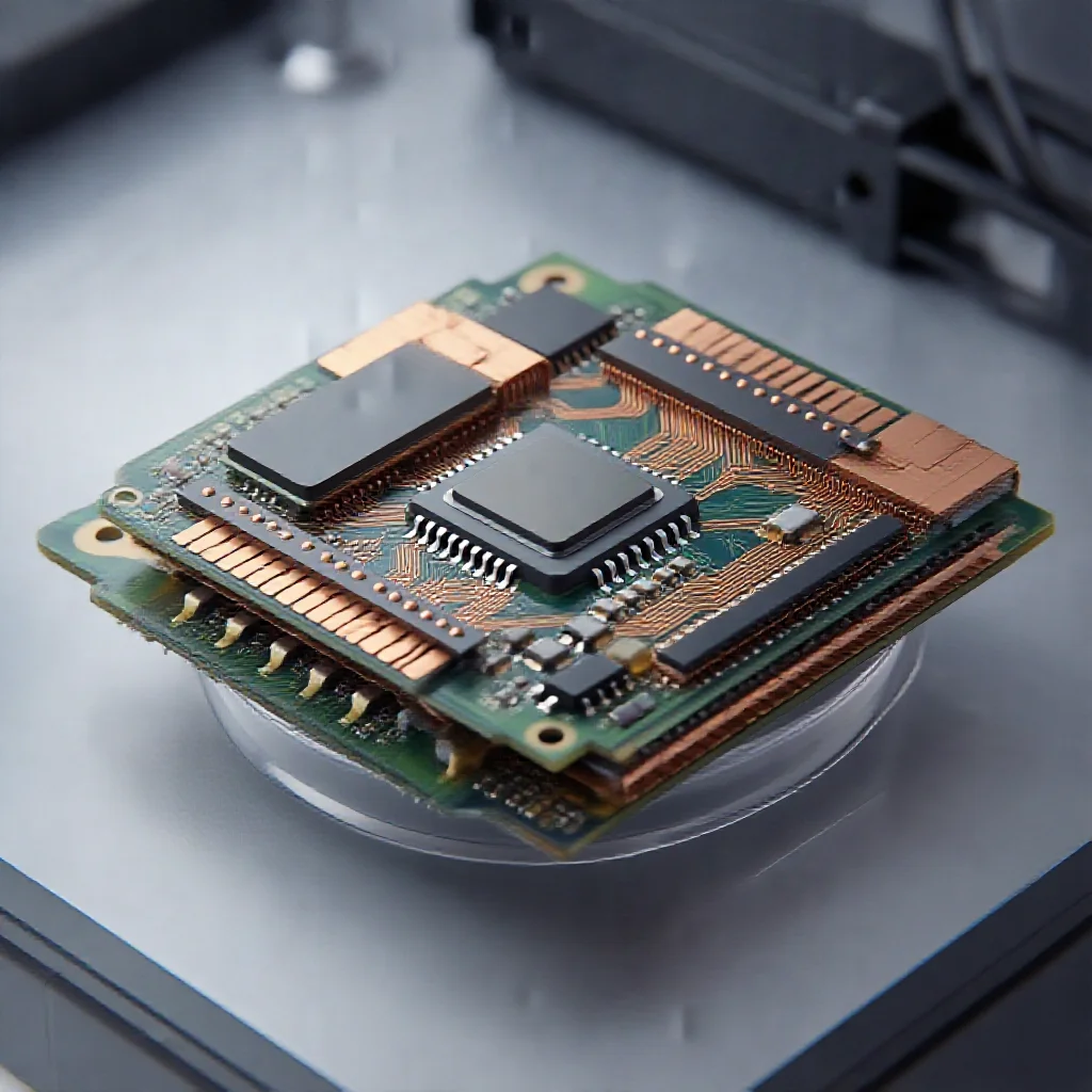
The New AI Bottleneck: How Advanced Packaging Became the Critical Choke Point in the Global Supply Chain
Introduction: The Great Wall of Packaging
The primary constraint on the expansion of artificial intelligence compute is no longer the shrinking of transistors. It is the complex, three-dimensional architecture required to bind them together at scale. This shift represents a fundamental reordering of semiconductor production priorities. While record-breaking investments in new fabrication plants (fabs) continue, a severe shortage in advanced packaging capacity has emerged, creating a reported 12-18 month delay for leading-edge AI hardware. The critical battleground has moved from the front-end fabrication of silicon dies to the back-end integration of those dies into functional systems, through technologies like Chip-on-Wafer-on-Substrate (CoWoS) and 3D stacking.
The Anatomy of a Bottleneck: Why Packaging Became King
The technical demands of modern AI accelerators have transformed packaging from a final assembly step into a core engineering discipline. Advanced packaging, which involves integrating high-bandwidth memory (HBM) stacks with multiple logic dies in a single package, is now a more significant technical and logistical challenge than fabricating the individual chips. This integration is essential for achieving the data transfer speeds and energy efficiency required for large language models and other intensive workloads.
Nvidia Corporation has established a formidable strategic advantage by securing the majority of Taiwan Semiconductor Manufacturing Company's (TSMC) most advanced CoWoS packaging capacity. This pre-allocation has created a high barrier to entry for competitors, such as Advanced Micro Devices (AMD), whose ability to scale production of rival AI accelerators is directly constrained by available packaging slots. In contrast, Intel Corporation has developed its own advanced packaging technology, Foveros, but its capacity is vertically integrated and primarily serves Intel's internal product lines, lacking the scale and open-market availability of TSMC's CoWoS operations.
The CHIPS Act Blind Spot: Fabrication Without Integration
The U.S. CHIPS and Science Act, a $52 billion legislative package, has exposed a critical strategic gap in its effort to re-shore semiconductor manufacturing. The Act's funding is heavily weighted toward the construction of new front-end fabrication facilities. However, it provides insufficient focus and incentive for establishing a parallel, domestic ecosystem for the most advanced packaging.
This creates a "Taiwan Transit" problem. Silicon wafers produced at new U.S. fabs, such as TSMC's facility in Arizona scheduled to begin output in 2025, will still need to be shipped to Taiwan for CoWoS-level packaging before they can be integrated into finished systems. This requirement negates a core objective of the CHIPS Act: to build resilient, geographically diversified supply chains. A two-year gap is projected between the start of Arizona fab output in 2025 and the expected volume production of TSMC's Arizona advanced packaging facility in late 2027, representing a period of continued logistical vulnerability.
Geopolitical Calculus: The Packaging Power Play
In the current AI hardware cycle, control over advanced packaging capacity confers more immediate and tangible leverage than control over leading-edge fabrication nodes. While multiple companies operate at the cutting edge of transistor fabrication, the ecosystem for cutting-edge 2.5D and 3D integration is far more concentrated.
The timeline for TSMC's Arizona packaging facility, targeting late 2027 for volume production, therefore represents a geopolitical asset as much as a commercial investment. It is a node of future supply chain control. This dynamic is likely to catalyze a new national security objective among major economies: "packaging sovereignty." The result may be a wave of protectionist policies and subsidies aimed specifically at fostering domestic advanced packaging capabilities, mirroring the current race in fab construction.
Ecosystem Impact: Winners, Losers, and the AI Slowdown
The packaging bottleneck has a cascading effect across the technology ecosystem. The immediate winner is Nvidia, whose early capacity lock-in provides a significant moat. The primary loser is the broader AI industry, which faces constrained hardware supply, potentially slowing the pace of model development and deployment. Cloud service providers and large enterprises planning AI infrastructure expansions face extended lead times and higher costs.
The delay also impacts the competitive landscape. Companies like AMD and startups developing alternative AI accelerators find their market entry and scaling capabilities throttled not by their chip designs, but by their access to packaging. This bottleneck may incentivize increased investment in alternative packaging architectures and suppliers, but building such capacity requires significant capital and time.
Conclusion: The Race to Package
The shift of the primary bottleneck from fabrication to packaging marks a new phase in the semiconductor industry. It reveals that manufacturing supremacy is no longer a single-dimensional race for transistor density, but a multi-dimensional contest encompassing design, fabrication, and integration. The 12-18 month delay currently observed is a market signal of this structural imbalance.
The strategic response is taking shape. The construction of TSMC's packaging facility in Arizona is a direct, though delayed, answer. Intel's continued investment in Foveros represents a second, vertically integrated track. Market projections suggest that while the current acute shortage may ease as new capacity comes online post-2027, advanced packaging will remain a high-value, concentrated segment of the supply chain. The companies and nations that successfully build and control these integration capabilities will hold significant influence over the next decade of computational progress.
Keywords

Layla Ibrahim
Technology Reporter covering fintech, AI, and startup ecosystems in the Gulf.