Beyond the Silicon: How Nvidia''s CoWoS Lockdown Reshapes the AI Supply Chain
The AI chip shortage is not just about transistors; it's about packaging. A critical bottleneck in TSMC's advanced CoWoS (Chip-on-Wafer-on-Substrate) packaging capacity is throttling global AI development. Nvidia's strategic move to secure a dominant share of this capacity has created a two-tier market, forcing competitors to scramble and exposing a fundamental vulnerability in the semiconductor supply chain. This article analyzes how this packaging choke point shifts power dynamics, impacts AI innovation beyond just hardware giants, and forces a strategic re-evaluation of supply chain dependencies for the entire tech industry.
Layla Ibrahim
Editorial Analyst
Beyond the Silicon: How Nvidia's CoWoS Lockdown Reshapes the AI Supply Chain
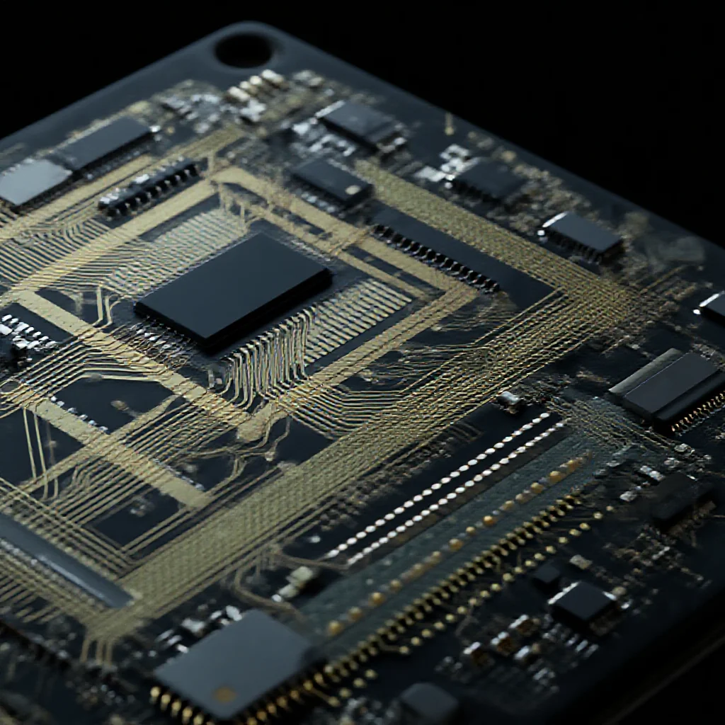
Image: A macro view of advanced semiconductor packaging, highlighting the intricate interconnects that have become a critical bottleneck.
Introduction: The Hidden Choke Point in the AI Gold Rush
The narrative of the artificial intelligence hardware shortage has predominantly focused on transistor fabrication at the world’s most advanced semiconductor foundries. However, the primary constraint throttling global AI development has shifted downstream. The critical bottleneck is not in etching patterns onto silicon wafers but in the "final mile" of manufacturing: advanced packaging. Specifically, the scarcity of TSMC’s CoWoS (Chip-on-Wafer-on-Substrate) packaging capacity is now the decisive factor governing the supply of high-performance AI accelerators. This packaging technology is essential for assembling the complex, multi-chiplet designs and integrating high-bandwidth memory (HBM) that define modern AI chips like GPUs. The strategic capture of this capacity by a single dominant player, Nvidia, is reconfiguring power dynamics across the technology industry.
Deconstructing the Bottleneck: Why CoWoS is the New Battleground
The technical demands of AI compute have rendered traditional chip packaging obsolete. CoWoS is a 2.5D advanced packaging solution that allows multiple silicon dies, or "chiplets," and stacks of HBM to be integrated onto a single interposer substrate. This creates a unified, high-bandwidth communication pathway between logic and memory, which is non-negotiable for training large language models. The process is capital-intensive and requires specialized expertise that extends beyond conventional fab operations.
While building new fabrication plants (fabs) captures headlines, expanding CoWoS capacity presents a distinct set of challenges. It involves procuring and calibrating specialized tooling, developing new materials, and mastering complex thermal and mechanical integration processes. TSMC has established a near-monopoly in providing this specific, high-volume advanced packaging service for leading-edge AI chips. Competitors like Samsung and Intel are developing alternative packaging technologies (e.g., Samsung’s I-Cube, Intel’s EMIB), but they lack the proven volume scale and ecosystem trust that TSMC’s CoWoS commands. This creates a significant time lag—estimated at 12-18 months—for meaningful competitive capacity to come online, during which demand continues to accelerate exponentially.
Nvidia's Strategic Gambit: Securing the AI Supply Chain's 'Lifeline'
Nvidia’s move to secure a dominant share of TSMC’s CoWoS output (Source 1: [Industry Analyst Reports]) transcends a simple large purchase order. It is a strategic capacity lockdown that functions as a formidable competitive moat. By committing capital upfront and collaborating deeply with TSMC on capacity planning, Nvidia has effectively guaranteed supply for its datacenter GPU families (Hopper, Blackwell). This action has direct, asymmetric consequences for the market.
Competitors, including AMD with its MI300 series and numerous custom silicon startups, now operate with severe uncertainty regarding their access to the necessary packaging. This has precipitated the emergence of a two-tier AI hardware market. Tier 1 consists of Nvidia and its closest partners, who have predictable access to the "lifeline" of CoWoS capacity. Tier 2 encompasses all other players, who must compete for the residual, unallocated packaging capacity, facing longer lead times and potential allocation cuts. This dynamic grants Nvidia not only product superiority but also supply chain supremacy.
The Ripple Effect: Consequences Beyond Hardware Availability
The implications of this packaging choke point extend far beyond quarterly shipment figures.
Innovation Stifling: Limited access to advanced packaging directly slows the iteration cycles of Nvidia’s competitors. The ability to rapidly prototype, test, and scale new chiplet architectures is constrained. This creates a feedback loop where architectural dominance is reinforced by supply chain control, making it profoundly difficult for alternative designs to gain market traction.
The Hyperscaler Dilemma: The situation validates the strategic foresight of cloud hyperscalers—Google, Amazon, and Microsoft—in developing in-house AI accelerators (TPU, Trainium, and Maia, respectively). While these companies also rely on TSMC for fabrication, their vertical integration provides greater leverage and insulation. However, it also forces them to diversify their advanced packaging strategies, seeking partnerships with Intel Foundry Services or Samsung to mitigate concentration risk, a clear indicator of the bottleneck’s severity.
The Startup Squeeze: For AI chip startups, the CoWoS shortage presents an existential threat. Their business models are predicated on accessing leading-edge foundry and packaging services as a "merchant" customer. With capacity locked down by incumbents, these startups face prohibitive barriers to scaling production, chilling venture investment and potentially consolidating innovation around a handful of well-capitalized entities.
The Long-Term Reconfiguration: Reshaping Global Semiconductor Strategy
The CoWoS bottleneck is forcing a fundamental re-evaluation of supply chain dependencies across the technology sector. It exposes a critical vulnerability: over-reliance on a single node (TSMC) for a highly specialized, capacity-constrained process. The logical market response is a multi-pronged strategic shift.
First, significant capital investment is being directed toward expanding advanced packaging capabilities globally. TSMC is accelerating its own expansion, while Intel and Samsung are marketing their packaging technologies as competitive alternatives. Second, chip architects are incentivized to design for packaging diversity, creating chiplets that can be assembled using multiple interoperable packaging technologies, though this adds complexity. Third, national industrial policies, such as the U.S. CHIPS Act, are now explicitly factoring advanced packaging into their funding priorities, recognizing it as a pillar of semiconductor resilience.
The long-term trajectory suggests a gradual diversification of the advanced packaging landscape. However, for the next 24-36 months, the constraint will remain acute. During this period, competitive advantage in AI will be determined not solely by transistor design or software ecosystems, but by the secured ability to physically assemble and deliver the final product. The era where packaging was an afterthought has conclusively ended; it is now a primary arena for strategic competition and a defining limiter on the pace of global AI adoption.
Keywords

Layla Ibrahim
Technology Reporter covering fintech, AI, and startup ecosystems in the Gulf.